English | MP4 | AVC 1280×720 | AAC 48KHz 2ch | 3h 08m | 635 MB
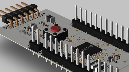
Designing printed circuit boards (PCBs)—which help to power nearly all electronic devices—requires both sound reasoning and creative thinking. In this course, Kirsch Mackey steps through this process, demonstrating how to design and output a PCB using OrCAD (also known as Allegro), the industry-leading software used by many of the world’s top electronic and consumer device manufacturers. Kirsch steps through how to work with both OrCAD Capture and PCB Editor to bring your project to the finish line, helping you become familiar with the electronic board development workflow along the way. Learn how to create electronic schematics, lay out your circuits on printed circuit boards, and generate manufacturing files and PCB documentation.
Topics include:
- Differences between OrCAD Capture and PCB Editor
- Starting a new project in Capture
- Organizing schematic parts
- PCB design in PCB Editor
- Manufacturing and design constraints
- Troubleshooting design errors
- Generating PCB documentation
Table of Contents
Introduction
1 Become comfortable and proficient in OrCAD
Getting Started
2 OrCAD Capture and PCB Editor differences
3 Setting up OrCAD for project success
4 Navigating and using OrCAD Capture
Schematic Design in Capture
5 Starting a new project in Capture
6 Add part libraries to a Capture project
7 Search and place parts in a schematic
8 Organize schematic parts
9 Connect the parts in the schematic
10 Schematic Design Rules Check (DRC)
11 Rename the parts (Annotate)
12 Check parts and finalize schematics
13 Generate a bill of materials (BOM)
14 Generate a smart PDF
15 Transfer a schematic to a PCB
PCB Design in PCB Editor
16 Navigation in PCB Editor
17 Setting up the PCB environment
18 Place the PCB outline and mounting holes
19 Placing components on the PCB
20 Manufacturing and design constraints
21 Routing the PCB, part 1
22 Routing the PCB, part 2
23 How to fix PCB footprint errors
24 Design Rules Check (DRC) and 3D collisions
Final Outputs
25 Drafting PCB information
26 Generate manufacturing files
27 Generate PCB documentation
Conclusion
28 End of design and next steps
Resolve the captcha to access the links!